Cloud Foundry Service for Post-Silicon Chip Prototyping
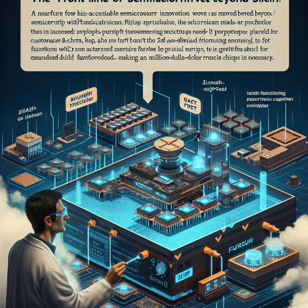
The next wave of chip innovation is moving beyond silicon, but most fabrication tools and foundries remain locked in a silicon-first world. Startups and academic labs working with 2D materials like bismuth oxyselenide lack access to prototyping services tailored to these new architectures. This startup would offer a cloud-accessible foundry-as-a-service, purpose-built for post-silicon transistor R&D. Users can upload GAAFET or 2D transistor designs, simulate behavior, and receive low-volume physical chips. It’s a mix of SaaS and fab-light services. Why now? China just demonstrated the world’s fastest transistor not based on silicon—this marks a turning point. A new wave of designers and material scientists will need faster iteration loops. Example: A university researcher developing a bismuth-based neuromorphic processor uploads a design and gets 20 test chips back in 10 days—no $10M cleanroom needed.
Description
No additional description provided.
The Pitch
In the realm of semiconductor technology, the landscape is evolving at an unprecedented pace. Traditional silicon-based technologies have dominated for decades, but the horizon is broadening to encompass advanced materials such as bismuth oxyselenide and other 2D materials. These materials are crucial for the next wave of chip innovation, promising higher efficiency and novel functionalities. However, startups and academic laboratories focusing on these new materials encounter significant barriers in terms of prototyping and fabrication. Most available fabrication tools and foundries are optimized for silicon, creating a bottleneck for post-silicon development.
**The Problem**
As the semiconductor industry veers towards these new materials, the existing infrastructure fails to support agile development and experimentation. Startups and research institutions often lack the means to prototype their designs without investing extensively in $10M cleanroom facilities and silicon-centric foundries. This slows down innovation and iteration cycles when speed is of the essence. With the recent demonstration of the world's fastest non-silicon-based transistor by China, it's clear that the industry must pivot quickly to keep pace with global advancements.
**The Solution**
Imagine a cloud-accessible foundry-as-a-service, specifically crafted for the post-silicon era of transistor research and development. This service would enable users to upload their Gate-All-Around Field-Effect Transistor (GAAFET) or 2D transistor designs, perform simulations, and receive low-volume, high-quality physical chips in a matter of days. The solution combines elements of Software as a Service (SaaS) with a fab-light approach, empowering innovators with the tools they need without the prohibitive cost and infrastructure requirements.
**Product Details**
The core offering of this service includes:
- **Design Upload and Simulation**: A user-friendly cloud platform where designers can upload their chip designs and run detailed simulations to predict behavior and performance. - **Prototyping Services**: Access to advanced fabrication technologies tailored for 2D materials, providing quick turnaround for low-volume chip production. - **Data Analysis and Optimization**: Built-in analytics tools to help users refine designs based on fabrication and test data. - **Integration and Testing**: Optional services to integrate and test chips within broader systems for functionality validation.
**Tools to Launch the MVP**
To launch this minimum viable product efficiently, the following tools and partners should be considered:
- **Cloud Infrastructure**: Utilize platforms like AWS or Google Cloud for hosting the SaaS component, ensuring scalability and security. - **Simulation Software**: Partner with leading software providers to integrate cutting-edge simulation tools into the platform. - **Fabrication Partners**: Collaborate with existing fab-light facilities or advanced research labs that have experience with 2D materials. - **Frontend and UX Design**: Implement a seamless, intuitive user interface to facilitate easy access and navigation.
**Go-to-Market Strategy**
A targeted GTM strategy will focus on:
- **Academic Institutions and Research Labs**: Engage with universities and research centers working on advanced materials, offering educational partnerships and discounted access for pilot studies. - **Startups in Semiconductor Innovation**: Network within the semiconductor startup community to showcase the benefits of rapid prototyping and collaborate on early-stage projects. - **Industry Conferences and Journals**: Present at key industry events and publish in relevant journals to build credibility and visibility. - **Strategic Alliances**: Form partnerships with materials suppliers or larger semiconductor firms aiming to diversify into post-silicon technologies.
**Business Model**
The business model blends SaaS with infrastructure services:
- **Subscription Model**: Charge a monthly or annual fee for access to the simulation and design upload platform. - **Per-Prototype Fee**: Charge an additional fee based on the number of physical chips produced, offering tiered pricing for different levels of complexity and volume. - **Professional Services**: Optional consulting and integration services for more tailored support, which can drive additional revenue.
This innovative approach positions the startup at the forefront of next-generation semiconductor development, offering much-needed resources to those pushing the boundaries of what's possible beyond silicon.